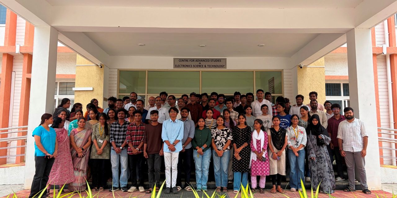
The Centre for Advanced Studies in Electronics Science and Technology (CASEST), University of Hyderabad, has officially kicked off two intensive, three-week internship programmes running from 1 July to 21 July 2026. Aimed at bridging the gap between classroom theory and industry reality, these programmes are training the next generation of tech pioneers in#VLSL Design and Semiconductor Fabrication Techniques.
With 40 students diving into VLSI and 20 hands-on in the fabrication labs, these cohorts are gaining exclusive, practical experience with state-of-the-art Electronic Design Automation (EDA) tools and cutting-edge cleanroom facilities.
The two specialized tracks offer an uncompromised, deep dive into the semiconductor lifecycle:
VLSI Design (Coordinated by Dr. Anjali Priya): Participants are mastering the complete Integrated Circuit (IC) design flow across both Digital and Analog domains. From RTL design, synthesis, and Static Timing Analysis (STA) to custom analog layouts and FPGA hardware implementation, students aren’t just learning—they are building. The programme culminates in a hardware-integrated mini-project.
Semiconductor Fabrication (Coordinated by Dr. S. L. D. Varma): Running in collaboration with the Centre for Nanotechnology, this track puts students inside a real cleanroom environment. Interns are getting hands-on with lithography, thin-film deposition, and etching. By the end of the three weeks, every single intern will have fabricated and tested their own Thin Film Transistor (TFT) on a Gallium Arsenide (GaAs) substrate.
Prof. Samrat Sabat, Head of CASEST, extended his congratulations to the coordinators for bringing these highly specialized programmes to life. He said, “Such initiatives are essential for developing a skilled workforce capable of contributing to India’s rapidly expanding semiconductor ecosystem. CASEST remains committed to offering high-quality experiential learning opportunities that bridge the gap between academic education and industry requirements.”